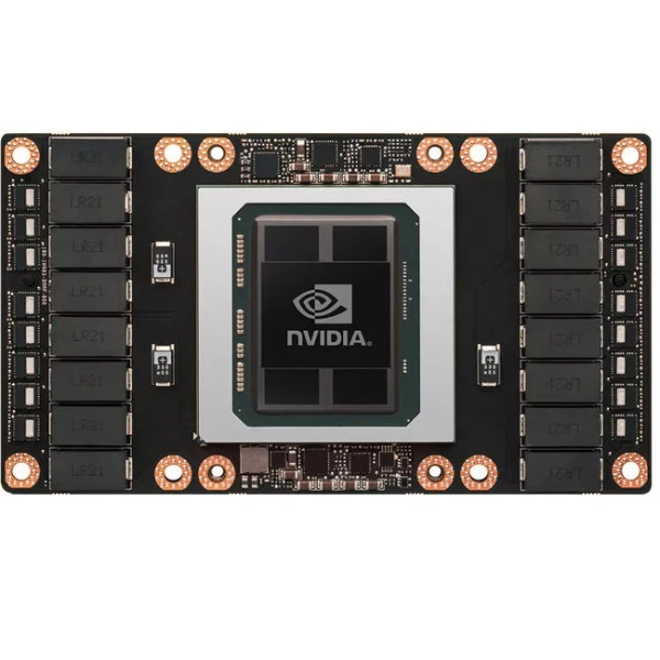
NVIDIA Tesla P100 SXM2

- Graphics Processor: GP100
- TMUs: 224
- Memory Type: HBM2
- Bus Width: 4096 bit
- ROPs: 96
NVIDIA Tesla P100 SXM2 Specs
NVIDIA’s professional graphics card, the Tesla P100 SXM2, was released on April 5, 2016. The GP100-890-A1 model of the card, which is based on the GP100 graphics processor and is built on the 16 nm technology, supports DirectX 12. The GP100 graphics processor is a big chip with 15,300 million transistors and a die area of 610 mm². It has 96 ROPs, 224 texture mapping units, and 3584 shading units. The Tesla P100 SXM2 and NVIDIA’s 16 GB HBM2 memory are linked by a 4096-bit memory interface. Memory operates at 715 MHz, while the GPU operates at 1328 MHz, with the possibility of increasing to 1480 MHz.
The NVIDIA Tesla P100 SXM2, a sxm module card, has a maximum power consumption rating of 300 W and doesn’t require an additional power connector. Since this device is not made to be linked to monitors, it does not have display connectivity. A PCI-Express 3.0 x16 interface is used to link the Tesla P100 SXM2 to the rest of the system.
Specifications
BASIC GPU INFO
| GPU name | GP100 |
| Manufacturer | NVIDIA |
| Released date | Apr 5th, 2016 |
| Launch price | $249 |
| Foundry | TSMC |
| Purpose | gaming |
| GPU codename | GP100-890-A1 |
| Generation | Tesla Pascal (Pxx) |
| Production | Discontinued |
| Successor | Tesla Volta |
| Predecessor | Tesla Maxwell |
BOARD DESIGN
| TDP | 300 W |
| Slot width | SXM Module |
| Power connectors | N/A |
| Outputs | No outputs available on this GPU |
| Board number | PH403 SKU 201 |
GRAPHICS PROCESSING UNIT
| Base clock | 1328 MHz |
| Boost clock | 1480 MHz |
| Transistors | 15,300 million |
| Process size | 16 nm |
| Die size | 610 mm² |
| Chip package | BGA-2621 |
| Density | 25.1M / mm² |
GPU MEMORY
| Memory type | HBM2 |
| Memory size | 16 GB |
| Memory bus | 4096 bit |
| Bandwidth | 732.2 GB/s |
| Memory clock | 715 MHz 1430 Mbps |
| Memory speed | N/A |
GRAPHICS FEATURES (API)
| Vulkan | 1.3 |
| DirectX | 12 (12_1) |
| OpenGL | 4.6 |
| OpenCL | 3.0 |
| Shader model | 6.0 |
| CUDA | 6.0 |
CONFIGURATION
| ROPs | 96 |
| Shading units | 3584 |
| TMUs | 224 |
| L1 cache | 24 KB (per SM) |
| L2 cache | 4 MB |
GPU PERFORMANCE
| Pixel rate | 142.1 GPixel/s |
| Texture rate | 331.5 GTexel/s |
| FP16 (half) | 21.22 TFLOPS (2:1) |
| FP32 (float) | 10.61 TFLOPS |
| FP64 (double) | 5.304 TFLOPS (1:2) |
FULL VIDEO REVIEW
Share your thoughts
Disclaimer Note
We can not guarantee that the information on this page is 100% correct.


