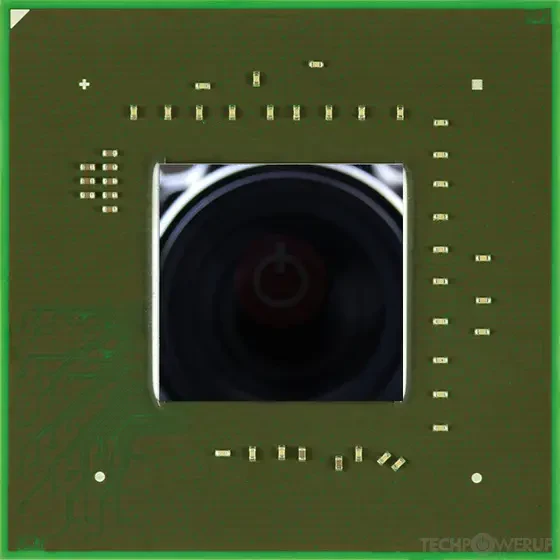
NVIDIA GeForce GTX 860M OEM

- Graphics Processor: GM107
- TMUs: 40
- Memory Type: GDDR5
- Bus Width: 128 bit
- ROPs: 16
NVIDIA GeForce GTX 860M OEM Specs
There is no need for an extra power connector because the NVIDIA GeForce GTX 860M OEM has a maximum power demand of 75 W. This GPU does not allow display connectivity because it is not meant to be connected to a monitor. Rather, it is intended for use in laptops and notebooks and will utilise the output of the host mobile device.
NVIDIA released the GeForce GTX 860M OEM, a mobile graphics chip, on February 5, 2015. The N15P-GX-A1 form of the chip, which is based on the GM107 graphics processor and is constructed using the 28 nm technology, supports DirectX 12. The feature level is only 11_0, which can cause issues with more recent DirectX 12 games, despite the fact that it supports DirectX 12. With 1,870 million transistors and a die area of 148 mm2, the GM107 graphics processor is a chip of typical size. It has 16 ROPs, 40 texture mapping units, and 640 shading units. Using a 128-bit memory interface, NVIDIA has linked the GeForce GTX 860M OEM with 2,048 MB of GDDR5 RAM.
Specifications
BASIC GPU INFO
| GPU name | GM107 |
| Manufacturer | NVIDIA |
| Released date | Feb 5th, 2015 |
| Launch price | $349 |
| Foundry | TSMC |
| Purpose | gaming |
| GPU codename | N15P-GX-A1 |
| Generation | GeForce 800M |
| Production | Discontinued |
| Successor | GeForce 900M |
| Predecessor | GeForce 700M |
BOARD DESIGN
| TDP | 75 W |
| Slot width | MXM Module |
| Power connectors | N/A |
| Length | N/A |
| Height | N/A |
| Width | N/A |
| Outputs | Portable Device |
| Board number | E2704 SKU 10 |
| Weight | N/A |
| Bus interface | MXM-B (3.0) |
GRAPHICS PROCESSING UNIT
| Base clock | 1097 MHz |
| Boost clock | 1176 MHz |
| Transistors | 1,870 million |
| Process size | 28 nm |
| Die size | 148 mm² |
| Chip package | FCBGA-908 |
| Density | 12.6M / mm² |
GPU MEMORY
| Memory type | GDDR5 |
| Memory size | 2 GB |
| Memory bus | 128 bit |
| Bandwidth | 80.19 GB/s |
| Memory clock | 1253 MHz 5 Gbps |
GRAPHICS FEATURES (API)
| DirectX | 12 (11_0) |
| OpenGL | 4.6 |
| OpenCL | 3.0 |
| Display port | N/A |
| Shader model | 6.7 (5.1) |
| CUDA | 5.0 |
CONFIGURATION
| ROPs | 16 |
| Shading units | 640 |
| TMUs | 40 |
| L1 cache | 64 KB (per SMM) |
| L2 cache | 2 MB |
GPU PERFORMANCE
| Vertex rate | N/A |
| Pixel rate | 18.82 GPixel/s |
| Texture rate | 47.04 GTexel/s |
| FP32 (float) | 1.505 TFLOPS |
| FP64 (double) | 47.04 GFLOPS (1:32) |
FULL VIDEO REVIEW
Share your thoughts
Disclaimer Note
We can not guarantee that the information on this page is 100% correct.


