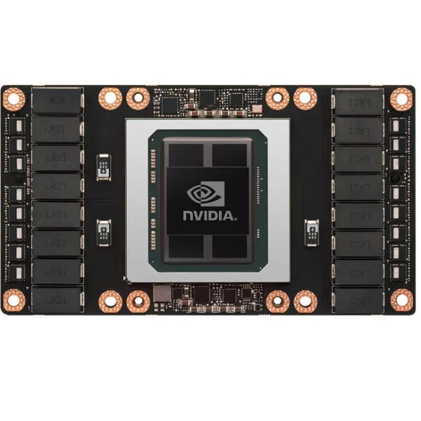
NVIDIA Tesla P100 SXM2 vs AMD Radeon 880M


| |
| Price | $249.00 |
| Our Rating | |
| Brand | NVIDIA AMD |
| Category | GPU Benchmarks GPU Benchmarks |
BASIC GPU INFO
| GPU name | GP100 Strix Point |
| Manufacturer | NVIDIA AMD |
| Released date | Apr 5th, 2016 Jul 2024 |
| Launch price | $249 |
| Foundry | TSMC TSMC |
| Purpose | gaming gaming |
| GPU codename | GP100-890-A1 |
| Generation | Tesla Pascal (Pxx) Navi III IGP (Strix Point Mobile) |
| Production | Discontinued Available |
| Successor | Tesla Volta |
| Predecessor | Tesla Maxwell Navi III IGP |
BOARD DESIGN
| TDP | 300 W 15 W |
| Slot width | SXM Module IGP |
| Power connectors | N/A N/A |
| Length | N/A |
| Width | N/A |
| Outputs | No outputs available on this GPU Portable Device Dependent |
| Board number | PH403 SKU 201 |
| Bus interface | PCIe 4.0 x8 |
GRAPHICS PROCESSING UNIT
| Base clock | 1328 MHz 400 MHz |
| Boost clock | 1480 MHz 2900 MHz |
| Transistors | 15,300 million 34,000 million |
| Process size | 16 nm |
| Die size | 610 mm² 233 mm² |
| Chip package | BGA-2621 FP8 |
| Density | 25.1M / mm² 145.9M / mm² |
GPU MEMORY
| Memory type | HBM2 System Shared |
| Memory size | 16 GB System Shared |
| Memory bus | 4096 bit System Shared |
| Bandwidth | 732.2 GB/s System Dependent |
| Memory clock | 715 MHz 1430 Mbps System Shared |
| Memory speed | N/A |
GRAPHICS FEATURES (API)
| Vulkan | 1.3 1.3 |
| DirectX | 12 (12_1) 12 Ultimate (12_2) |
| OpenGL | 4.6 4.6 |
| OpenCL | 3.0 2.1 |
| Shader model | 6.0 6.8 |
| CUDA | 6.0 |
CONFIGURATION
| ROPs | 96 16 |
| Shading units | 3584 512 |
| TMUs | 224 32 |
| RT Cores | 12 |
| Compute units | 12 |
| L1 cache | 24 KB (per SM) 128 KB per Array |
| L2 cache | 4 MB 2 MB |
GPU PERFORMANCE
| Vertex rate | N/A |
| Pixel rate | 142.1 GPixel/s 46.40 GPixel/s |
| Texture rate | 331.5 GTexel/s 92.80 GTexel/s |
| FP16 (half) | 21.22 TFLOPS (2:1) 5.939 TFLOPS (2:1) |
| FP32 (float) | 10.61 TFLOPS 2.970 TFLOPS |
| FP64 (double) | 5.304 TFLOPS (1:2) 185.6 GFLOPS (1:16) |


|


