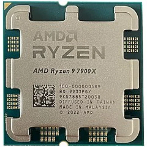
AMD Ryzen 7 9700X

- Cores: 8
- TDP: 65 W
- Socket: Socket AM5
- Codename: Granite Ridge
- Frequency: 3.8 GHz
AMD Ryzen 7 9700X Benchmark
The Ryzen 7 9700X uses normal power levels for a contemporary PC, with a TDP of 65 W. AMD’s CPU has a dual-channel interface that supports DDR5 memory. Although 5600 MT/s is the maximum officially supported memory speed, overclocking (together with the appropriate memory modules) allows for even faster performance. Additionally, ECC memory is available, which is a crucial feature for mission-critical systems to prevent data corruption. A PCI-Express Gen 5 connection is used by the Ryzen 7 9700X to communicate with other parts of the computer. The Radeon Graphics integrated graphics solution is a feature of this CPU.
With 32 MB of L3 cache, the Ryzen 7 9700X runs at 3.8 GHz by default, but depending on the workload, it may go to 5.5 GHz. AMD is constructing the Ryzen 7 9700X with 8,315 million transistors on a 4 nm manufacturing technology. Instead of AMD, TSMC’s foundry fabricates the chip’s silicon die.
Launched in August 2024, the AMD Ryzen 7 9700X is an 8-core desktop CPU with an MSRP of $359. It uses the Zen 5 (Granite Ridge) architecture with Socket AM5 and is a member of the Ryzen 7 range.
Specifications
BASIC CPU INFO
| Foundry | TSMC |
| Manufacturer | Amd |
| Generation | Ryzen 7 (Zen 5 (Granite Ridge) |
| Socket | AMD Socket AM5 |
| Package | FC-LGA1718 |
| Status | Available |
| Process size | 6 nm |
| Die size | 70.6 mm² |
| tMax | 95°C |
CPU PERFORMANCES
| Base clock | 100 MHz |
| Turbo clock | up to 5.5 GHz |
| Frequency | 3.8 GHz |
PROCESSOR FEATURES
| Part# | 100-000001404 |
| Multiplier | 38.0x |
| Memory support | DDR5 |
CHIP ARCHITECTURE
| Codename | Granite Ridge |
| Memory support | DDR5 |
| DDR5 speed | 5600 MT/s |
| ECC memory | Yes |
| Chipset | X870E, X870, B850, B840, X670E, X670, B650E, B650, A620 |
| PCl - express | Gen 5, 24 Lanes (CPU only) |
SYSTEM CONFIGURATION
| Integrated graphics | Radeon Graphics |
| # of cores | 8 |
| # of threads | 16 |
| SMP #CPUs | 1 |
CACHE HIERARCHY
| Cache L0 | N/A |
| Cache L1 | 80 KB (per core) |
| Cache L2 | 1 MB (per core) |
| Cache L3 | 32 MB (shared) |
Share your thoughts
Disclaimer Note
We can not guarantee that the information on this page is 100% correct.


