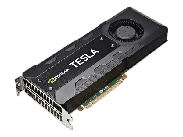
NVIDIA Tesla K40c

NVIDIA Tesla K40c
$7,699.00
Brand: NVIDIA
Category: GPU Benchmarks
  • Graphics Processor: GK180
  • TMUs: 240
  • Memory Type: GDDR5
  • Bus Width: 384 bit
  • ROPs: 48

SpecsByte Rating

Official Specs Rating: "Expert evaluation based on authentic manufacturer specifications and detailed product datasheets."

6.2
  • Gaming 5 / 10
  • Memory and Bandwidth 7 / 10
  • Power Consumption 7 / 10
  • Performance 6 / 10
  • Temperature and Noise 6 / 10
  • Value for money 6 / 10

NVIDIA Tesla K40c Specs

NVIDIA released the Tesla K40c, a professional graphics card designed for enthusiasts, on October 8, 2013. The card, in its GK180-890-A1 model, supports DirectX 12 and is based on the GK180 graphics processor and the 28 nm technology. A huge device with 7,080 million transistors and a die area of 561 mm² is the GK180 graphics processor. In addition to 48 ROPs, it has 240 texture mapping units and 2880 shading units. The Tesla K40c and 12 GB of GDDR5 memory have been matched by NVIDIA and are connected via a 384-bit memory interface. While the GPU operates at 745 MHz, with the potential to increase to 876 MHz, the RAM operates at 1502 MHz (6 Gbps effective).

With a maximum power consumption rating of 245 W, the NVIDIA Tesla K40c is a dual-slot card that uses one 6-pin and one 8-pin power connector. Since it is not intended to be linked to a monitor, this device does not support display connectivity. Using a PCI-Express 3.0 x16 interface, the Tesla K40c is linked to the rest of the system. With a dual-slot cooling solution, the card is 267 mm long. When it was first released, it cost 7699 USD.
Specifications

BASIC GPU INFO

GPU name GK180
Manufacturer TSMC
Released date Oct 8th, 2013
Launch price $7,699
Architecture Kepler
Generation Tesla Kepler (Kxx)
Production End-of-life
Successor Tesla Maxwell

BOARD DESIGN

TDP 245 W
Slot width Dual-slot
Power connectors 1x 6-pin + 1x 8-pin
Length N/A
Height N/A
Width N/A
Outputs No outputs available on this GPU
Board number P2081 SKU 206

GRAPHICS PROCESSING UNIT

Base clock 745 MHz
Boost clock 876 MHz
Transistors 7,080 million
Process size 28 nm
Die size 561 mm²
Chip package BGA-2152
Density 12.6M / mm²

GPU MEMORY

Memory type GDDR5
Memory size 12 GB
Memory bus 384 bit
Bandwidth 288.4 GB/s
Memory clock 1502 MHz 6 Gbps more effective

GRAPHICS FEATURES (API)

Vulkan 1.2.175
DirectX 12 (11_0)
OpenGL 4.6
OpenCL 3.0
Display port N/A
Shader model 5.1
Ray tracing N/A

CONFIGURATION

ROPs 48
Shading units 2880
TMUs 240
Compute units N/A
L1 cache 16 KB (per SMX)
L2 cache 1536 KB

GPU PERFORMANCE

Pixel rate 52.56 GPixel/s
Texture rate 210.2 GTexel/s
FP16 (half) N/A
FP32 (float) 5.046 TFLOPS
FP64 (double) 1.682 TFLOPS (1:3)

Share your thoughts

  • Be the first to add a Review

    Please post a user review only if you have / had this product.

Disclaimer Note

We can not guarantee that the information on this page is 100% correct.